
086-769-81605596
1106, Jinlong Bldg., Xiaobian, Chang'an Town, Dongguan, Guangdong, China (Mainland)


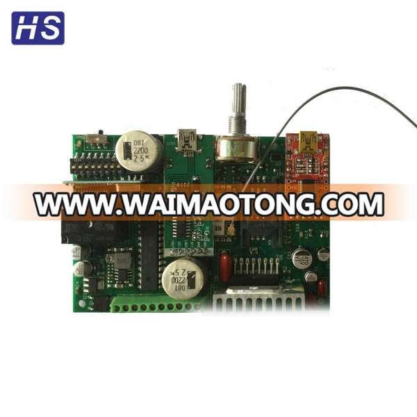
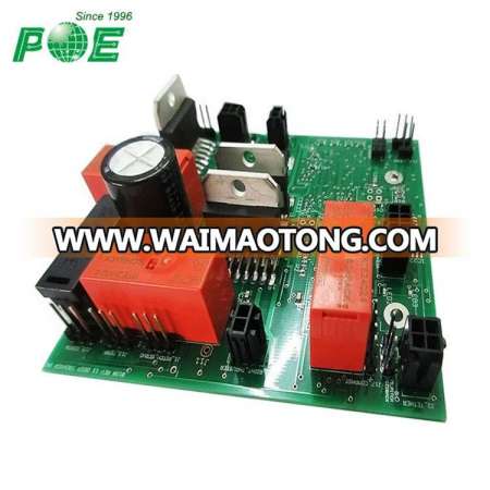
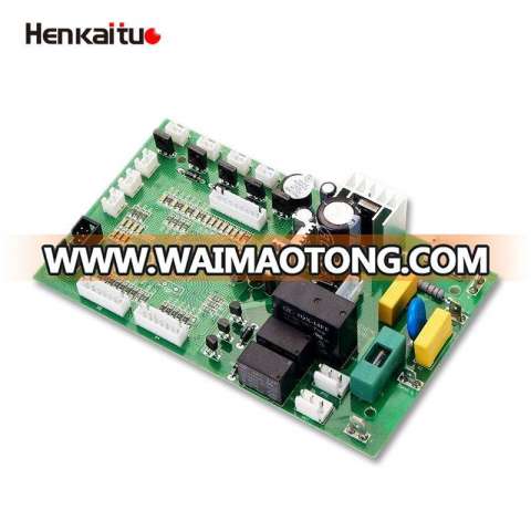
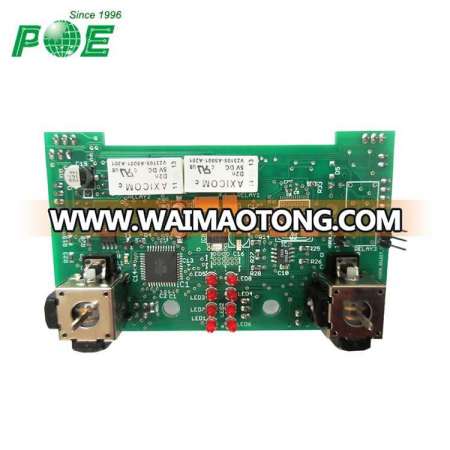
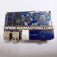
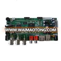
Pcb /pcba Design,Bom Gerber Files Multilayer Pcb,Prototype Pcb , Find Complete Details about Pcb /pcba Design,Bom Gerber Files Multilayer Pcb,Prototype Pcb,Pcb Board,Electronics Pcb Pcba,Pcb Manufacturer from Other PCBPCBA Supplier or Manufacturer-Shenzhen Hansion Technology Co., Ltd.
We can do for you:
♦ 1-12 layer FR4 PCB.
♦ 1-2layer aluminum PCB.
♦ 1-4layer flexible PCB.
♦ CEM-1 PCB
♦ 94VO PCB
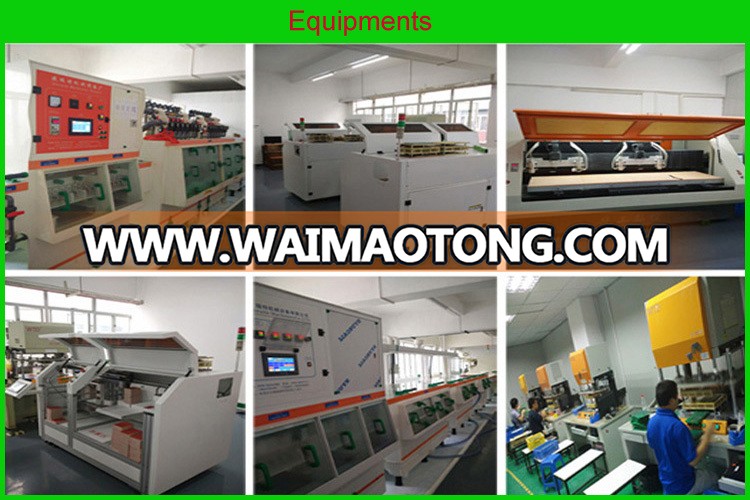
♦ SMT and DIP assembly service.

FAQ:
Q:1.Can i have a sample to test?
A:Yes,we can send you samples to test.
Q:2.What specifications do you need for PCB quotation?
A:We need your PCB Gerber file,board thickness,copper thickness,surface finishing and quantity to quote you.
Q:3.What is the lead time?
A:Samples need 3-5days,mass production needs 7-10days,also according to the order volume.
Q:4.Do you have MOQ limit?
A:Even 1 pcs,we care.
Q:5.Can you offer the best price for us?
A:Yes,we are specialized PCB manufacturer directly,we can offer lower price than any trading company.
Q:6.How do you ship the goods and how long does it take arrival?
A:We usually ship by DHL,UPS,FedEx and TNT.It takes 3-5days to arrive.
Q:7.What are the payment terms?
A:You can pay us with Paypal,Western Union and T/T Bank.
Q:8.Can we visit your factory?
A:Yes,welcome to visit our factory anytime,and we will lead you to visit our factory and our production line.
Manufacturing Capability:
item | Manufacture Capability |
Material | FR4,CEM-1, Aluminium, Polyamide |
Layer No. | 1-12 |
Finished board thickness | 0.1 mm-4.0mm |
Board Thickness Tolerance | ±10% |
Cooper thickness | 0.5 OZ-3OZ (18 um-385 um) |
Copper Plating Hole | 18-40 um |
Impedance Control | ±10% |
Warp&Twist | 0.70% |
Peelable | 0.012"(0.3mm)-0.02’(0.5mm) |
Images | |
Min Trace Width (a) | 0.075mm (3mil) |
Min Space Width (b) | 0.1mm (4 mil) |
Min Annular Ring | 0.1mm (4 mil) |
SMD Pitch (a) | 0.2 mm(8 mil) |
BGA Pitch (b) | 0.2 mm (8 mil) |
Solder Mask | |
Min Solder Mask Dam (a) | 0.0635 mm (2.5mil) |
Solder mask Clearance (b) | 0.1mm (4 mil) |
Min SMT Pad spacing (c) | 0.1mm (4 mil) |
Solder Mask Thickness | 0.0007"(0.018mm) |
Holes | |
Min Hole size (CNC) | 0.2 mm (8 mil) |
Min Punch Hole Size | 0.9 mm (35 mil) |
Hole Size Tol (+/-) | PTH:±0.075mm;NPTH: ±0.05mm |
Hole Position Tol | ±0.075mm |
Plating | |
HASL | 2.5um |
Lead free HASL | 2.5um |
Immersion Gold | Nickel 3-7um Au:1-5u'' |
OSP | 0.2-0.5um |
Outline | |
Panel Outline Tol (+/-) | CNC: ±0.125mm, Punching: ±0.15mm |
Beveling | 30°45° |
Gold Finger angle | 15° 30° 45° 60° |
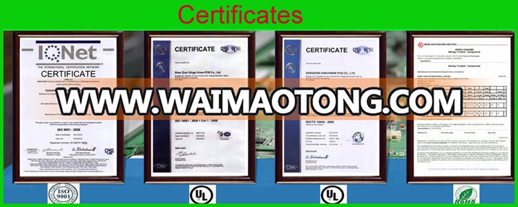
Certificate | ROHS, ISO9001:2008, SGS, UL certificate |


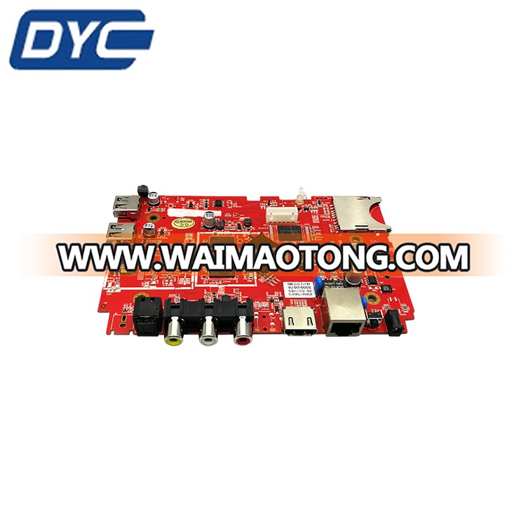
Lcd tv pcb main board,OEM/SMT PCBA/PCB Assembly /Electronics components
Electronic Customized PCBA Manufacturer, OEM PCB Assembly, SMT/DIP PCBA Assembly
13 YEARS OEM ODM Shenzhen SMD PCB Assembly Manufacture LED PCBA
China custom made PCB manufacturing and Assembly electronic PCBA
PCB design, schematic and pcba design, electronic product design
Fast PCB Copy Prototype & PCBA Prototype Service from PCB PCBA Manufacturer SATECH